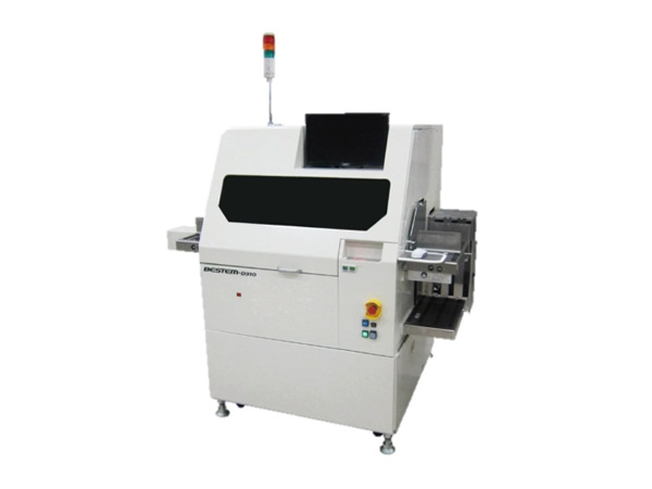
Epoxy Die BonderBESTEM-D310/D311plus

- Overview
- D310 Specifications
- D311plus Specifications
Basic Information
Model name : BESTEM-D310/D311plus
Twin-dispenser die bonder for 8-inch wafer IC·LSI
Features
1. Equipped with a twin-dispenser system to improve productivity
2. Achieves high quality by minimizing the distance between bond application and chip mounting to suppress changes in the adhesive over time
3. Equipped with wizard functionality to realize excellent operability
4. Equipped with a back-side recognition camera to realize high accuracy (D311plus)
Main Specs
- Bonding Method
- Epoxy bonding
- Coating unit
- Twin-dispenser method
- Bonding Speed
- 0.180sec/cycle
*Not including processing time
- Bonding Accuracy
-
XY: ±25 μm, 3 σ
θ: ±1°, 3 σ (□1.0 mm or above)
θ: ±3°, 3 σ (Less than □1.0 mm)
- Die Size
-
□0.3-□8.0 mm
t: 0.1-0.5 mm
Option: □0.15-2.0 mm
- Lead frame size
(substrate size) -
Length: 50-260 mm
(as an option, supports up to 300 mm)
Width: 20-102 mm
Thickness: 0.1-1 mm
(as an option, supports up to 3 mm)
- Wafer Size
- Max φ8 inch
- Power requirements
-
Power requirements: AC200V 15A
Dry air: 0.4MPa (60L/min)
Vacuum source: -66.7kPa (100L/min)
- Dimensions
-
(W) 1,860 × (D) 1,282 × (H) 1,622mm
(without signal tower when front cover is closed)
- Weight
- Approximately 1,500 kg
Options
- Optional Functions
-
1. Wafer mapping
2. Traceability
3. Needleless pickup
*1. Device size may vary depending on options.
2. Changes in the quality standards may be requested depending on the specifications of the applicable products.
3. Please note that the specifications are subject to change without notice.
Main Specs
- Bonding Method
- Epoxy bonding
- Coating unit
- Twin-dispenser method
- Bonding Speed
-
0.300sec/cycle Back-side recognition ON
0.248sec/cycle Back-side recognition OFF
*Not including processing time
- Bonding Accuracy
-
Back-side recognition ON:
XY: ±15 μm, 3 σ
θ: ±1°, 3 σ (□1.0 mm or above)
θ: ±3°, 3 σ (Less than □1.0 mm)
Back-side recognition OFF
XY: ±25 μm, 3 σ
θ: ±1°, 3 σ (□1.0 mm or above)
θ: ±3°, 3 σ (Less than □1.0 mm)
- Die Size
-
□0.3-□8.0 mm
(Option: □0.15-2.0 mm)
t:0.1-0.5 mm
When back-side recognition is supported: □0.3-2.5 mm
(Option: □0.1-0.7 mm)
- Lead frame size
(substrate size) -
Length: 50-260 mm
(as an option, supports up to 300 mm)
Width: 20-102 mm
Thickness: 0.1-1 mm
(as an option, supports up to 3 mm)
- Wafer Size
- Max φ8 inch
- Power requirements
-
Power requirements: AC200V 15A
Dry air: 0.4MPa (60L/min)
Vacuum source: -66.7kPa (100L/min)
- Dimensions
-
(W) 1,860 × (D) 1,282 × (H) 1,622mm
(without signal tower when front cover is closed)
- Weight
- Approximately 1,500 kg
Options
- Optional Functions
-
1. Wafer mapping
2. Traceability
3. Needleless pickup
*1. Device size may vary depending on options.
2. Changes in the quality standards may be requested depending on the specifications of the applicable products.
3. Please note that the specifications are subject to change without notice.


 简体中文
简体中文 日本語
日本語 English