

 简体中文
简体中文 日本語
日本語 English
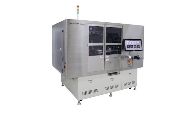
DAF High-Accuracy Die BonderBESTEM-D631
- Overview
- Specifications
Basic Information
Model name : BESTEM-D631
High-accuracy die bonder for NAND flash memory compatible with 12-inch wafers.
Features
1. Realizes high-accuracy bonding with a linear motor drive head and image processing alignment at an intermediate stage
2. Equipped with a high-accuracy image processing recognition system to realize high-accuracy position inspection
3. Equipped with a chip crack inspection function for use in chip recognition, intermediate stage recognition, and bonding island recognition
4. Equipped with an automatic collet replacement function and a position correction function
Main Specs
- Bonding Method
- Thermal compression bonding (WL-DAF)/DAF tape
- Bonding Speed
-
1.03 sec/chip
*Not including processing time
- Bonding Accuracy
-
XY: ±7 μm, 3 σ
θ: ±0.05°, 3 σ
±0.1°, 3 σ (chips with edge lengths of 3 mm or less)
- Die Size
-
□1.0 -18.0 mm
t: 0.025-1.0 mm
- Lead frame size
(substrate size) -
Length: 100-315 mm
Width: 45-115 mm
Height: 50-200 mm
- Wafer Size
- Max φ12 inch
- Power requirements
-
Power requirements: AC200V 20A
Dry air: 0.5MPa (150L/min)
Vacuum source: -66.7kPa (100L/min)
- Dimensions
-
(W) 2422 × (D) 1727.5 × (H) 2332mm
(without signal tower when front cover is closed)
- Weight
- Approximately 2,000 kg
Options
- Optional Functions
-
1. Support for automation
2. Support for chip crack inspection
3. Support for collet foreign substance inspection
4. Support for chip height detection
*1. Device size may vary depending on options.
2. Changes in the quality standards may be requested depending on the specifications of the applicable products.
3. Please note that the specifications are subject to change without notice.